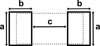
This drawing shows the typical sizes of a land pattern for SMD resistors. The length of the pads is indicated by ‘a’, width of the pad by ‘b’ and the gap between the solder pads by ‘c’.
This drawing shows the typical sizes of a land pattern for SMD resistors. The length of the pads is indicated by ‘a’, width of the pad by ‘b’ and the gap between the solder pads by ‘c’.